- July 23 2025
Modern military power depends less on raw firepower and more on computational superiority. At the heart of this shift lies an unassuming but critical component: the printed circuit board (PCB). These intricate networks of copper and substrate form the central nervous system of every advanced weapons system, communications device, and surveillance platform deployed by modern armed forces.
Unlike commercial electronics designed for climate-controlled offices or consumer pockets, military PCBs operate in environments that would cripple ordinary circuitry. They must maintain flawless operation while enduring:
- Extreme temperatures (from -55°C in Arctic deployments to 125°C near jet engines)
- Mechanical shock (artillery recoil, carrier deck landings, parachute drops)
- Electromagnetic interference (both natural and weaponized)
- Chemical/biological exposure (from desert sand to decontamination fluids)
The technological demands extend beyond ruggedization. Modern defense PCBs incorporate:
- Radiation-hardened components for nuclear scenarios
- Tamper-proof architectures to prevent reverse engineering
- Low-observable materials for stealth applications
This combination of extreme reliability and advanced functionality makes military PCBs fundamentally different from their commercial counterparts. Where consumer electronics prioritize cost and time-to-market, defense applications demand:
- Decade-long product lifecycles with guaranteed component availability
- MIL-SPEC certification for every material and process
- Redundant designs that degrade gracefully under partial failure
The strategic implications are profound. A fighter jet’s radar superiority, a missile’s targeting precision, or a drone’s autonomous capabilities all ultimately depend on the quality and innovation embedded in its circuit boards. As warfare becomes increasingly networked and electronic, PCB technology has quietly emerged as a key determinant of military effectiveness, one that combines materials science, electrical engineering, and strategic foresight.
The Five Critical Military PCB Applications

Military PCBs operate where failure is not an option. Across air, land, sea, and space systems, these specialized circuit boards perform mission-critical functions under conditions that would destroy commercial electronics.
Avionics: The Brain of Modern Aircraft
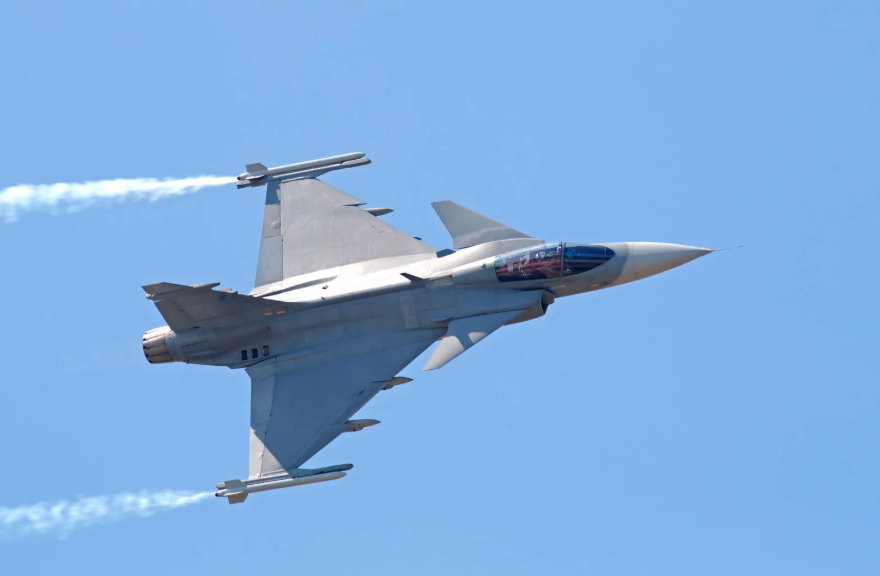
Fighter jets like the F-35 contain some of the most advanced PCB technology on Earth. Their avionics systems process radar returns, manage flight controls, and execute electronic warfare tactics, all while withstanding 9G maneuvers and extreme temperature swings. These boards use polyimide or PTFE substrates for stable high-frequency operation, with components mounted using underfill adhesives to prevent vibration-induced failures. The F-35’s APG-81 radar alone contains over 1,500 specialized PCBs working in concert.
Precision Guidance Systems
Modern munitions achieve their accuracy through sophisticated PCB stacks. A single Javelin missile guidance system combines:
- MEMS gyroscope interface boards
- Millimeter-wave radar processors
- Electro-optical sensor arrays
All packaged to survive 20,000G launches while maintaining nanosecond-level timing precision. These designs increasingly use system-in-package (SiP) technology to minimize size without sacrificing reliability.
Secure Communications Architecture
Military radios and encryption devices employ PCBs with physical security features that commercial manufacturers never consider. Tamper-resistant designs might include:
- Mesh sensors that erase cryptographic keys if breached
- Faraday cage layers are screen-printed between PCB strata
- Self-destruct mechanisms triggered by intrusion attempts
The NSA’s Type 1 encryption devices take this further, with entire PCB layers dedicated to detecting and responding to physical tampering in real-time.
Unmanned Systems Electronics
Predator drones and autonomous ground vehicles push PCB technology in opposing directions, demanding both miniaturization and extreme ruggedness. Their circuit boards must:
- Process multiple HD video streams simultaneously
- Maintain secure datalinks in contested RF environments
- Operate for days without maintenance
This requires careful balancing of high-density interconnect (HDI) techniques with military-grade conformal coatings and vibration-resistant component mounting.
Warfighter Wearables
Today’s soldiers carry more computing power than entire command centers did in the 1990s. Modern infantry electronics integrate:
- Heads-up displays with waveguide PCBs
- Vital signs monitors with flexible circuits
- Secure GPS/IRIDIUM communicators
All packaged to survive mud, impacts, and electromagnetic pulses while drawing minimal power. The U.S. Army’s Nett Warrior system exemplifies this, with its central computing module using a 22-layer rigid-flex PCB measuring just 3cm square.
The Manufacturing Edge Behind Military-Grade PCBs

Producing circuit boards for defense applications requires not only tightened tolerances, but also a complete rethinking of PCB fabrication processes to meet extreme reliability and security requirements. Military PCB manufacturing operates on a different plane from commercial production, where every material, process, and supplier must adhere to stringent military specifications.
Material selection forms the foundation of military PCB capability. While consumer electronics rely on cost-effective FR-4, defense systems increasingly turn to specialized substrates like Rogers RO4000 series for high-frequency radar applications or Arlon 85N for thermal management in power electronics. These materials maintain stable dielectric constants across temperature extremes while resisting the moisture absorption that could compromise performance in humid environments. For the most demanding applications, manufacturers employ ceramic-filled PTFE blends that can handle millimeter-wave frequencies up to 110GHz, which is critical for advanced electronic warfare systems.
The fabrication process itself incorporates multiple layers of redundancy and verification. Laser-direct imaging replaces traditional photolithography to achieve the 25μm line/space resolutions needed for high-density designs, with each layer undergoing automated optical inspection at 10x magnification. Through-hole plating exceeds standard thickness by 25-50% to ensure reliability under thermal cycling, while microvias are filled with conductive epoxy to prevent void formation. Conformal coatings get applied in controlled-environment chambers, with thickness verified by X-ray fluorescence to guarantee complete coverage of all components.
Testing and qualification separate military PCB production most dramatically from commercial practices. Boards undergo environmental stress screening that includes:
- Thermal shock cycling between -55°C and 125°C
- 96-hour salt spray exposure
- Random vibration testing replicating helicopter transport
- High-potential testing at 1500V DC
Radiation-hardened versions for space systems face additional proton and gamma ray exposure tests. Each of these evaluations follows strict MIL-PRF-31032 or MIL-PRF-55110 protocols, with full traceability of all test results.
Supply chain security completes the military PCB ecosystem. Defense contractors maintain approved vendor lists with audited facilities, while sensitive designs often require US-only fabrication with component-level DNA marking to prevent counterfeiting. The most critical programs employ blockchain-based material tracking from mine to finished assembly, a necessity when a single substandard capacitor could compromise a multi-million-dollar weapons system. This comprehensive approach to manufacturing transforms ordinary circuit boards into the resilient neural networks of modern military platforms.
The Next Frontier in Military PCB Technology
Military PCB development is entering its most transformative phase since the transition to surface-mount technology. Three groundbreaking innovations are redefining defense electronics’ capabilities while introducing new strategic considerations.
Additive manufacturing has evolved beyond prototyping to enable mission-specific circuit integration. Lockheed Martin’s recent demonstration of 3D-printed conformal electronics embedded in missile wings represents a paradigm shift. By depositing conductive traces directly onto structural components using aerosol jet printing, engineers achieved a 40% weight reduction compared to traditional PCB assemblies while eliminating geometric constraints. The Army Research Lab is pushing this further with self-healing conductive polymers that automatically repair minor ballistic damage. This capability could extend the operational lifespan of field-deployed electronics.
Quantum computing threats are driving revolutionary changes in secure PCB architectures. Current research focuses on optical interconnect layers that eliminate vulnerable electrical signal paths, along with physically unclonable functions (PUFs) fabricated directly into PCB substrates. These PUFs generate unique cryptographic keys based on microscopic variations in the board’s material structure, making each unit inherently tamper-resistant. DARPA’s SHIELD program takes physical security further, developing chips with microscopic fluid channels that permanently disable the device if removed from its original PCB.
Artificial intelligence is transforming both the design and operational capabilities of military PCBs. Machine learning algorithms now optimize board layouts for electromagnetic resilience, predicting and mitigating interference patterns that human engineers might miss. Northrop Grumman recently employed AI-driven design tools to reduce a critical radar system’s layer count from 18 to 12 while simultaneously improving thermal performance. This achievement directly translates to weight savings and reliability improvements. In operational systems, embedded AI coprocessors enable real-time performance adaptation, allowing boards to compensate for damaged traces or degraded components in battlefield conditions.
These advancements collectively are enabling entirely new classes of military systems. From conformal electronics that merge with airframe structures to self-securing boards that actively resist cyber-physical attacks, the next generation of military PCBs will play an increasingly strategic role in national defense.
PCBs as a Strategic Advantage in Modern Warfare
The evolution of military PCBs has reached an inflection point where circuit board technology now directly influences combat effectiveness and geopolitical power balances. What began as simple interconnect platforms has become sophisticated systems that often determine the success or failure of entire weapons programs.
Three critical realities define this new paradigm:
Electronic Superiority Trumps Raw Firepower
The F-35’s radar cross-section, hypersonic missiles’ terminal guidance, and drone swarms’ coordination all depend on PCB innovations that outpace adversary capabilities. When seconds determine mission success, the quality of a board’s signal integrity or thermal management can prove more decisive than explosive yield.
Security Extends to the Physical Layer
Modern defense PCBs incorporate tamper-proofing that begins at the material level, self-destruct features, optical isolation, and component-level encryption. These measures recognize that sophisticated adversaries now attack supply chains and hardware as aggressively as they target software vulnerabilities.
Manufacturing Capability Equals Military Capability
Nations that master advanced PCB production, from radiation-hardened space electronics to AI-optimized designs, gain asymmetric advantages. The U.S. Department of Defense’s recent $2.3 billion investment in domestic PCB infrastructure underscores this strategic reality.
For engineers and defense contractors, these developments create both enormous responsibility and unprecedented opportunity. The circuit boards designed today will empower the defense systems of 2040 and beyond. Those who push boundaries in materials, security architectures, and manufacturing processes are shaping the future of national security.
The Path Forward
Maintaining leadership in military PCB technology requires:
- Continued investment in domestic manufacturing ecosystems
- Cross-disciplinary collaboration between materials scientists and defense engineers
- Agile adoption of commercial innovations (like AI design tools) for defense applications
The most consequential battles of future conflicts may well be decided by silent, uncelebrated victories in PCB laboratories and fabrication facilities. And Microchip USA’s custom PCB manufacturing service leverages world class fabs that can produce high-quality and robust PCB’s that meet defense requirements. We’re not just a manufacturer, we pride ourselves on delivering unequaled service to our partners, so contact us and request a quote today!